1
/
of
3
MTI Corporation
Graphene Film on Ni/SiO2/Si 100mm diameter
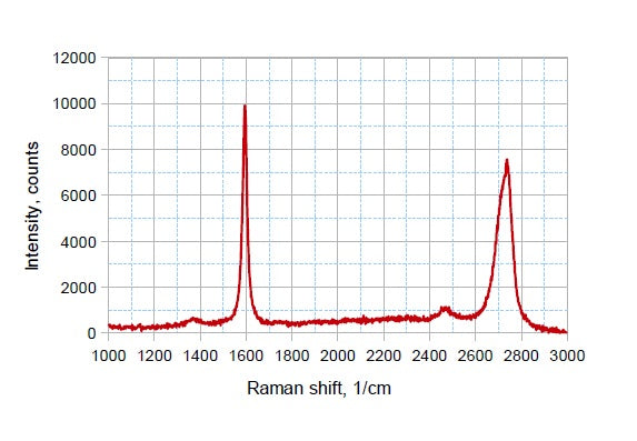
Graphene™ films are grown directly on a Ni/SiO2/Si deposited on an oxidized silicon wafer using a CVD process.
Specifications:
- Research Grade, about 90 % useful area
- Wafer Size: 100 mm diameter
- Growth Method:Chemical Vapor Deposition (CVD) Technique
- Film thickness: 1-10 monolayer thick
- Graphene film is multilayer with thickness varying in the range 1-10 layers;
- Graphene layers are aligned relative to each (graphite-like A-B stacking ) other as indicated by the Raman spectrum
- The graphene is grown on Ni film by CVD process.
- Nickel film is deposited on the substrate covered by thermally grown oxide layer
- Thickness of the Ni layer is 400 nm;
- The thickness of the silicon oxide layer is 500 nm;
- The thickness of the wafer is 500 μm
- The crystallographic orientation of silicon is 100;
- Films are continuous with low defect density.
- Atomically thin carbon film ( 1-10 layer )
- Outstanding electronic properties
- Chemical inertness and stability
- Unprecedented mechanical strength
MPN: FmGrapheneOnNiandSOandSi100US
Share


