Have an account?
Log in to check out faster.
Loading...
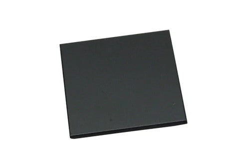
MTI Corporation
Device Layer
Size:
5mmx5mm
Type/Dopant:
N type/P-doped
Orientation:
<1-0-0>+/-0.5 degree
Thickness:
2.5±0.5µm
Resistivity:
1-4 ohm-cm
Finish:
Front Side Polished
Buried Thermal Oxide:
1.0 um +/- 0.1 um
Handle Wafers:
Type/Dopant
P type/B-doped
Orientation
10-20 ohm.cm
625 +/- 15 um
As received (not polished)
Be the first to know about new collections and exclusive offers.