-
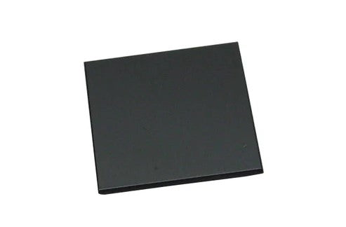
SOI Wafer:5x5x0.625mm, 2 .5"m (P-doped) +1.0 SiO2 +625um Si (P-type /Boron doped)
Specifications Specifications Device Layer Size: 5mmx5mm Type/Dopant: N type/P-doped Orientation: &...
Regular price $0.00Regular priceUnit price per -
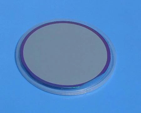
SOI Wafer: 6", 2.5 "m (P-doped ) + 1.0 SiO2 + 625um Si (P-type /Boron doped )
Specifications PSpecifications Device Layer Diameter: 6" Type/Dopant: N type/P-doped Orientation: ...
Regular price $0.00Regular priceUnit price per -
SOI Wafer: 10x10x0.625mm, 2.5um (P-doped) +1.0 SiO2 +625um Si (P-type/Boron doped)
Specifications Device Layer Size: 10x10 Type/Dopant: N type/P-doped Orientation: <1-0-0>+/-0....
Regular price $0.00Regular priceUnit price per